
The Brief
The News:
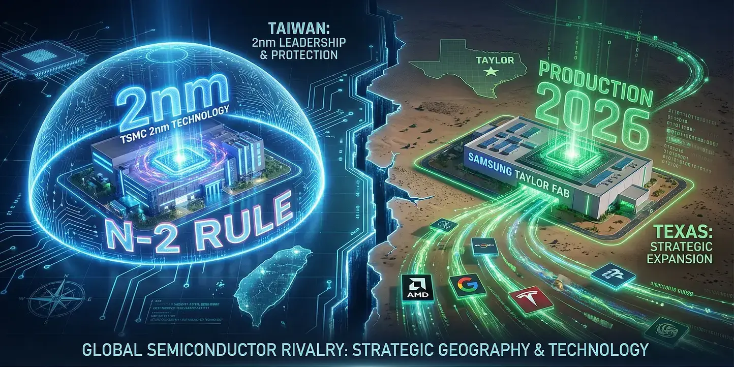
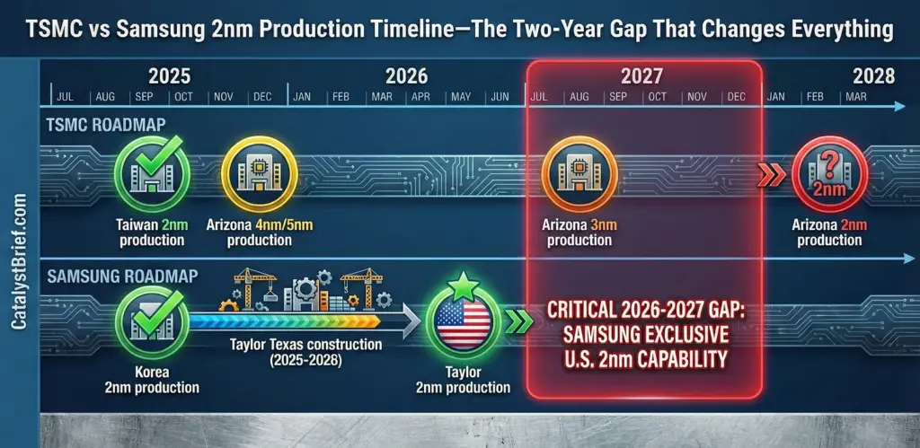
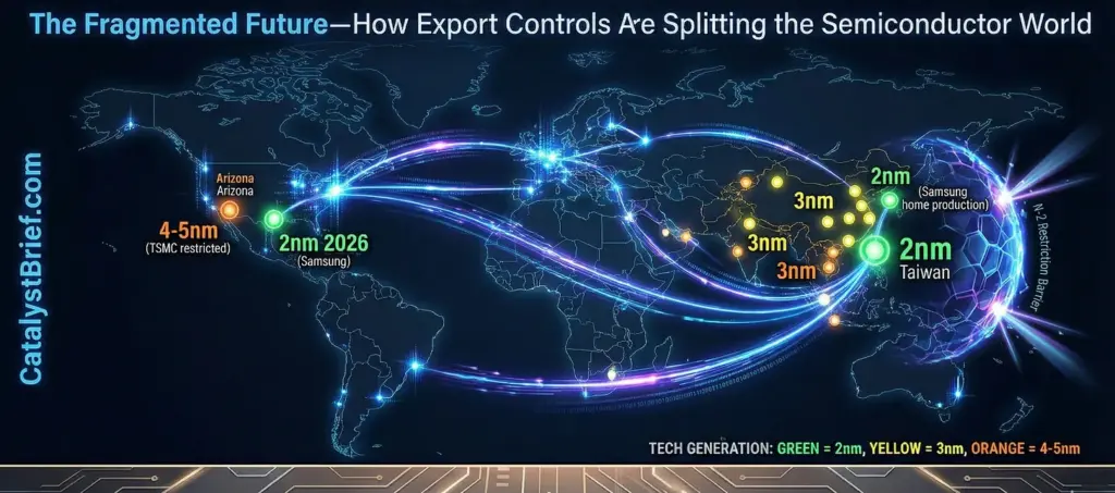
Taiwan’s National Science and Technology Council reaffirmed its N-2 export rule in December 2025, restricting TSMC from deploying its most advanced 2-nanometer chip technology at overseas facilities for at least two years. This means TSMC’s Arizona plant will not produce 2nm chips until at least 2027, while Samsung’s Taylor, Texas fab targets 2026 production.
The Stats:
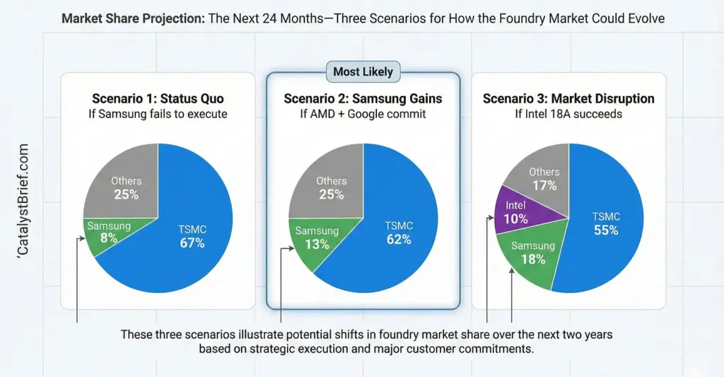
TSMC’s 2nm wafers cost approximately $30,000 USD each, while Samsung has undercut that price by 33% to $20,000 USD per wafer. Samsung’s Taylor fab construction reached 93.6% completion by the end of Q3 2025, with full completion targeted for July 2026. TSMC holds 67.6% of the global foundry market as of Q1 2025, while Samsung’s share stands at approximately 8%.
The Bottom Line:
A Taiwanese export control designed to protect national security is inadvertently creating the first real opening for Samsung to challenge TSMC’s dominance in advanced chip manufacturing. With nearly half of TSMC’s 2nm capacity already locked in by Apple, major U.S. tech companies including AMD, Google, and Tesla are now in active negotiations with Samsung for domestic 2nm production.
The Catalyst
In the high-stakes world of semiconductor manufacturing, geography has suddenly become destiny. Taiwan’s decision to enforce its N-2 export rule is reshaping the global chip supply chain in ways that policymakers likely never anticipated. While the regulation was designed to protect Taiwan’s technological crown jewels, it has inadvertently handed Samsung Electronics what may be the biggest strategic opportunity in the company’s foundry history.
The N-2 rule is deceptively simple in its mechanism but profound in its implications. Under this framework, Taiwan permits TSMC to export only those manufacturing technologies that trail the island’s leading-edge production capabilities by at least two full generations. Deputy Minister Lin Fa-cheng of the National Science and Technology Council emphasized in December 2025 that this policy applies strict controls to protect core semiconductor research and development, with the list of restricted technologies reviewed annually.
For TSMC, which entered high-volume manufacturing of its N2 process in Taiwan in late 2025, this creates a significant timing problem. The company’s Arizona Fab 21 Phase 1 currently produces 4nm and 5nm chips. Phase 2, scheduled to begin manufacturing in 2027, was originally planned for 3nm production. However, because 3nm is formally just one generation behind the 2nm family, this violates the N-2 restriction. Even when TSMC does eventually receive permission to produce 2nm chips in Arizona, that won’t happen until at least 2027, and only after the company develops its next-generation Angstrom-era nodes at home in Taiwan
This regulatory constraint arrives at precisely the moment when demand for advanced chip manufacturing in the United States has reached fever pitch. The combination of geopolitical tensions around Taiwan, supply chain resilience concerns amplified by recent chip shortages, and the explosive growth of AI infrastructure has made domestic semiconductor production a matter of national security priority. The U.S. CHIPS and Science Act, which provides billions in subsidies and tax incentives for domestic fabrication, explicitly aimed to bring the most advanced manufacturing back to American soil. The N-2 rule directly undermines that objective by ensuring that TSMC’s U.S. facilities will perpetually lag two to four years behind the technological frontier.
Samsung has recognized this opening and moved aggressively to capitalize on it. The company’s $37 billion USD fabrication facility in Taylor, Texas represents one of the largest foreign direct investments in U.S. manufacturing history. By the end of the third quarter of 2025, construction had reached 93.6% completion, with the facility on track for full commissioning in July 2026. Unlike TSMC, Samsung faces no regulatory restrictions on deploying its most advanced process technologies overseas. This means the Taylor fab can begin producing 2nm chips using Samsung’s SF2P process as soon as the facility is ready, making it the only location in the United States capable of manufacturing leading-edge semiconductors in 2026.
The strategic value of this positioning cannot be overstated. For U.S. technology companies facing pressure to secure domestic supply chains, Samsung’s Texas facility offers something that TSMC’s Arizona plant cannot: access to the absolute cutting edge of silicon manufacturing on American soil. This is particularly critical for AI infrastructure, where the difference between process nodes directly translates into computational efficiency, power consumption, and ultimately, competitive advantage in the race to build and deploy large language models and autonomous systems
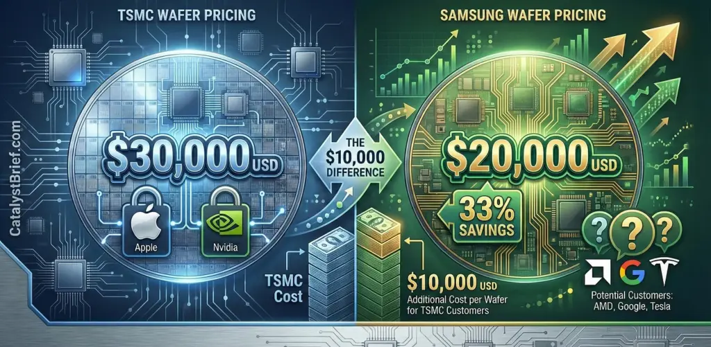
Samsung has not relied solely on geography to win business. The company has deployed an aggressive pricing strategy that undercuts TSMC by approximately 33%. While TSMC’s 2nm wafers are priced at around $30,000 USD each, representing a 10-20% increase over its 3nm process, Samsung has set its SF2 wafer pricing at approximately $20,000 USD. For companies designing chips that require thousands or tens of thousands of wafers, this $10,000 USD differential represents hundreds of millions in potential savings.
This pricing maneuver carries risk for Samsung. The company’s foundry division has struggled financially, with analysts estimating losses exceeding $3.6 billion USD in the first half of 2025 alone. Offering such steep discounts could further erode already thin margins. However, the alternative is arguably worse. Samsung has invested tens of billions in building advanced fabrication capacity in both South Korea and the United States, and that capacity has been running significantly below utilization due to a shortage of customer orders. In this context, aggressive pricing serves two purposes: it attracts immediate business to fill the fabs, and it builds long-term relationships with major technology companies that could yield sustained revenue for years to come.
The strategy appears to be working. In July 2025, Samsung announced a $16.5 billion USD contract with Tesla to produce the automaker’s next-generation AI6 chip at the Taylor facility. The deal, which runs through 2033, represents one of the largest foundry orders Samsung has ever secured from a single client. Tesla CEO Elon Musk confirmed that the Texas fab would be dedicated to manufacturing the AI6 processor, describing the strategic importance of the partnership as difficult to overstate. Musk even noted that he plans to personally walk the production line to accelerate progress, given the facility’s proximity to his residence.
Beyond Tesla, Samsung has secured significant design wins across multiple market segments. The company is currently producing Apple’s image sensor chips, custom mining ASICs for Chinese manufacturers MicroBT and Canaan, and its own Exynos 2600 application processor, which will power the Galaxy S26 flagship smartphone series launching in early 2026. More significantly, Samsung is in advanced negotiations with some of the biggest names in AI and computing
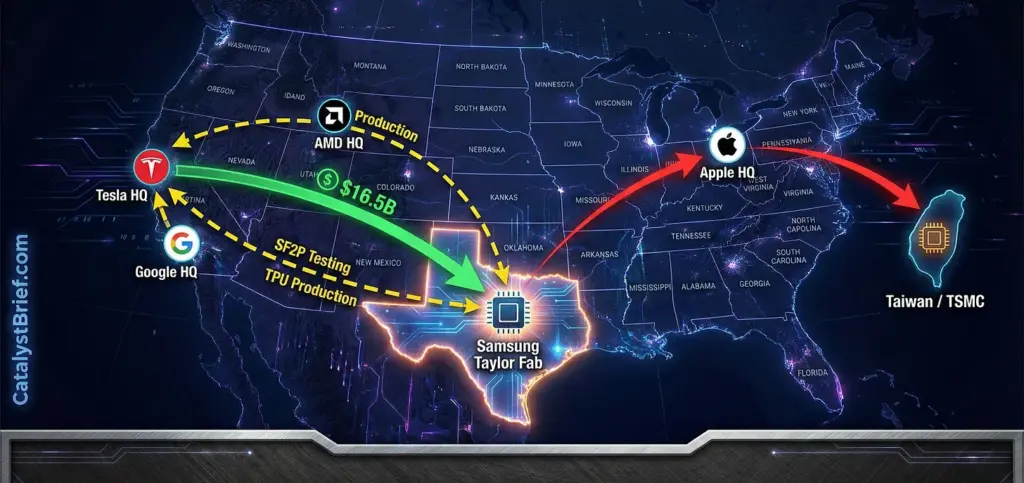
Reports from South Korean media in late December 2025 indicate that AMD and Google are in serious discussions with Samsung about 2nm chip production at the Taylor facility. Samsung Electronics Executive Chairman Lee Jae-yong personally met with AMD CEO Lisa Su during a recent trip to the United States to discuss foundry cooperation. Industry sources indicate that Samsung is running Multi-Project Wafer sample tests with AMD for its second-generation SF2P node, with a final decision on a formal contract expected around January 2026. AMD appears to be pursuing a dual-foundry strategy, continuing to use TSMC for its Zen 6 server CPUs while potentially shifting next-generation Ryzen processors to Samsung’s 2nm process to mitigate supply chain risk.
Google represents an even larger potential opportunity. The search and cloud computing giant has been designing custom Tensor Processing Units for its data centers, chips specifically optimized for AI workloads. According to industry sources, Google’s TPU team visited Samsung’s Taylor fab to discuss production capacity and volume commitments. As Google begins selling TPUs to external customers like Meta rather than reserving them exclusively for internal use, securing reliable high-volume manufacturing becomes critical. Samsung’s combination of U.S.-based production, competitive pricing, and 2026 availability makes it an attractive option for Google’s scaling plans.
These customer acquisition efforts come at a particularly opportune moment because TSMC’s capacity constraints are becoming increasingly acute. Industry analysts estimate that Apple has already reserved nearly half of TSMC’s initial 2nm production capacity for its A-series and M-series processors. Nvidia is reportedly planning to begin using TSMC’s 2nm process in 2027 for its next-generation graphics processors and AI accelerators. With two of the world’s most demanding chip buyers consuming the majority of available capacity, companies like Qualcomm, AMD, and Google face a stark choice: wait in line for TSMC’s limited remaining slots, or explore alternatives.
The technical specifications of Samsung’s 2nm process have been a point of debate within the semiconductor industry. Both TSMC and Samsung are transitioning to Gate-All-Around transistor architecture, a fundamental redesign that wraps the gate around all four sides of the channel to minimize current leakage. Samsung was actually the first to implement GAA technology at the 3nm node, though that early introduction was plagued by yield issues that damaged customer confidence. The company claims its second-generation SF2P process has achieved yields around 50-60%, a significant improvement from the low yields that characterized its 3nm ramp but still trailing TSMC’s reported 80% yields for N2
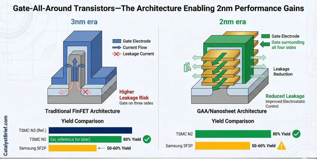
Some industry observers have questioned whether Samsung’s SF2 node should be considered a true 2nm process or rather an enhanced 3nm variant. The skepticism stems from the fact that transistor density and performance improvements appear more modest than the generational leap suggested by the naming convention. However, from a commercial perspective, the semantic debate over nomenclature matters less than the practical reality: Samsung can offer U.S. companies access to its most advanced process technology in Texas starting in 2026, while TSMC cannot.
The business implications extend beyond the United States. Taiwan’s N-2 policy creates a two-tier global supply chain where the most advanced chips can only be manufactured on the island itself. This fragmentation carries risks for the industry. If Nvidia continues relying exclusively on TSMC’s Taiwan facilities for its most powerful AI accelerators while AMD sources from Samsung’s U.S. fab, hardware capabilities could begin to diverge based purely on geographic and regulatory factors rather than engineering prowess. We may see scenarios where certain AI models or autonomous driving systems can only reach their full potential when deployed on chips manufactured in specific locations.
For Taiwan, the N-2 rule represents a careful balancing act. The island has long relied on its semiconductor manufacturing leadership as a form of economic and geopolitical insurance, the so-called Silicon Shield that makes Taiwan indispensable to the global economy. By keeping the most advanced manufacturing processes at home, Taiwan maintains leverage and ensures that any military aggression would come at an unacceptable economic cost to the global supply chain. However, this strategy also creates friction with Taiwan’s most important ally and security guarantor, the United States, which has spent billions attempting to bring advanced manufacturing back to American soil through the CHIPS Act.
The Center for Strategic and International Studies has noted that Taiwan’s N-2 policy directly conflicts with U.S. objectives to achieve true semiconductor independence. American policymakers envisioned facilities like TSMC’s Arizona fab producing the absolute leading edge, not technology that is two to four years behind. This tension is unlikely to be resolved easily, as both sides have legitimate security concerns driving their positions
Samsung’s window of opportunity, while significant, is not guaranteed to translate into long-term market share gains. The company has attempted to challenge TSMC’s foundry dominance before, most notably with its early adoption of 3nm GAA technology, only to stumble on execution. Major customers including Qualcomm and Google have previously shifted production away from Samsung to TSMC after experiencing yield problems and delays. Trust in the semiconductor foundry business is hard-won and easily lost.
The upcoming Exynos 2600 launch in the Galaxy S26 will serve as a critical real-world validation of Samsung’s 2nm manufacturing capabilities. If the chip delivers strong performance and efficiency while maintaining acceptable yields, it could provide the proof point needed to convince skeptical customers that Samsung has resolved its historical production challenges. Conversely, any significant issues would reinforce existing doubts and make it much harder to win business from risk-averse enterprise customers.
The competitive dynamics are also complicated by Intel’s aggressive push to revitalize its foundry business. Intel’s 18A process, which the company characterizes as equivalent to 1.8nm, is entering risk production in Arizona. Unlike TSMC, Intel is not bound by Taiwanese export restrictions and has pioneered backside power delivery with its PowerVia technology. If Intel can execute on its roadmap and achieve acceptable yields, it could emerge as a third option for U.S. companies seeking domestic advanced manufacturing, further fragmenting the market.
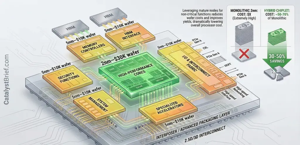
The economics of leading-edge semiconductor manufacturing continue to escalate in ways that could fundamentally reshape the industry. At $30,000 USD per wafer for TSMC’s 2nm process and $20,000 USD for Samsung’s equivalent, only the wealthiest corporations can afford to design and manufacture custom chips at these nodes. This concentration of capability is leading to what some analysts call the Economic Wall, where the barrier to entry for custom silicon rises so high that only a handful of Silicon Superpowers can participate.
This dynamic is already driving changes in chip design strategies. Rather than building entire processors on the most expensive 2nm nodes, companies are increasingly adopting chiplet architectures where only the most performance-critical compute dies use the leading edge, while less sensitive components remain on older, cheaper nodes. This approach can reduce costs by 30-50% while still delivering the performance benefits where they matter most for AI and high-performance computing workloads
Looking beyond 2nm, both TSMC and Samsung have already outlined roadmaps for 1.4nm and 1.6nm processes expected to enter production between 2027 and 2028. These future nodes will likely require High Numerical Aperture Extreme Ultraviolet lithography, a next-generation manufacturing technology that allows for even finer circuit patterns. The capital requirements for these advanced processes will be staggering, with individual fabrication facilities potentially costing $40-50 billion USD or more. Only companies with massive scale and deep financial resources will be able to participate.
For the AI industry specifically, the convergence of semiconductor manufacturing constraints and regulatory geography creates a complex planning environment. Companies building large language models and autonomous systems must make chip procurement decisions years in advance, committing to specific foundries and process nodes long before the technology is fully mature. The choice between TSMC’s Taiwan-only 2nm production, Samsung’s U.S.-based manufacturing, or waiting for Intel’s 18A process carries implications for everything from computational performance to supply chain resilience to regulatory compliance.
The geopolitical dimensions add another layer of complexity. As tensions between the United States and China continue to evolve, semiconductor manufacturing becomes increasingly intertwined with national security policy. Export controls, investment restrictions, and technology transfer regulations can change rapidly, making long-term planning challenging. Companies must balance pure technical and economic considerations with the political and regulatory landscape in ways that were uncommon just a few years ago.
Taiwan’s N-2 rule represents just one example of how governments are using semiconductor policy as a strategic tool. China has invested hundreds of billions in domestic chip manufacturing capabilities, though with mixed results at the leading edge. The European Union has launched major initiatives to increase semiconductor self-sufficiency. Japan is actively courting TSMC and other manufacturers to build advanced fabs on Japanese soil. Each of these efforts fragments what was once a relatively seamless global supply chain.
For Samsung, the current moment represents a genuine inflection point. The combination of favorable regulatory positioning, aggressive pricing, strategic geography, and TSMC’s capacity constraints creates conditions that may not persist indefinitely. If the company can execute technically, deliver on yield targets, and build trust with major customers, the Taylor fab could serve as the foundation for a sustained challenge to TSMC’s foundry dominance. The $16.5 billion USD Tesla contract provides both financial stability and a high-profile reference customer that could attract additional business.
However, success is far from guaranteed. TSMC’s manufacturing excellence, process technology leadership, and deep relationships with the world’s most important chip designers have been built over decades. While the N-2 rule creates a temporary advantage for Samsung in the U.S. market, TSMC is not standing still. The company continues to invest heavily in research and development, with roadmaps extending through the Angstrom era. TSMC’s yields consistently outperform competitors, and its ability to ramp new process technologies faster than anyone else in the industry remains a formidable competitive moat
The next 18 months will be critical. Samsung must prove it can deliver production-quality 2nm chips at volume from the Taylor fab while maintaining the yields and reliability that enterprise customers demand. AMD and Google’s decisions on whether to commit significant production volume to Samsung will signal how the broader industry views the company’s technical capabilities. The Exynos 2600 launch will provide visible evidence of whether Samsung has truly resolved its manufacturing challenges or if problems persist.
For technology professionals and investors watching this space, several key indicators will signal how the competitive landscape evolves. First, watch AMD’s formal announcement about its foundry strategy for next-generation Ryzen processors. A commitment to Samsung would validate the company’s 2nm process in the eyes of one of the most demanding chip designers in the industry. Second, monitor Google’s TPU production decisions. If Google shifts significant volume to Samsung, it would demonstrate that hyperscale cloud providers view the Taylor fab as a viable alternative to TSMC for AI workloads.
Third, pay attention to Samsung’s yield disclosures and any commentary from customers about production quality. Yields are the fundamental metric of manufacturing competence in the semiconductor industry, and sustained improvement would address the biggest historical concern about Samsung’s foundry business. Fourth, observe whether Qualcomm, which publicly canceled its Samsung 2nm Snapdragon project earlier in 2025, reconsiders that decision based on newer data about Samsung’s manufacturing capabilities.
The stakes extend beyond the immediate competitive dynamics between TSMC and Samsung. The fragmentation of advanced semiconductor manufacturing across geographic and regulatory boundaries has implications for innovation velocity, technology access, and global economic integration. If the most powerful AI systems can only be built using chips manufactured in specific locations due to regulatory restrictions, it could create new forms of digital divide and competitive imbalance.
The Catalyst’s Take
I predict that within 18 months, Samsung will have secured commitments from at least two of the big four hyperscalers (Google, Microsoft, Amazon, Meta) for TPU or custom AI accelerator production at the Taylor fab. The combination of U.S.-based manufacturing, competitive pricing, and TSMC’s capacity constraints creates a unique window of opportunity that these companies cannot ignore. While TSMC will maintain its overall market leadership, we’ll see the global foundry market shift from a near-monopoly to an oligopoly structure, with Samsung capturing 12-15% market share by 2027, up from 8% today. The real question isn’t whether Samsung will win significant business, but whether the company can sustain that business through multiple process generations or if this represents a temporary advantage that disappears once TSMC receives permission to manufacture 2nm in Arizona. The Exynos 2600 launch will be the first major test of whether Samsung has truly solved its yield problems or if history will repeat itself.Further Reading
Further Reading
- TSMC’s N-2 Geopolitical Hurdle: A Win for Samsung and Intel – Analysis of how Taiwan’s export controls are reshaping U.S. chip manufacturing
- The 2nm Sprint: TSMC vs. Samsung in the Race for Next-Gen Silicon – Deep dive into the technical specifications and competitive positioning
- Taiwan’s N-2 Rule Explained – Comprehensive explanation of the regulatory framework protecting Taiwan’s semiconductor technology
- Samsung, TSMC Set Stage for Fierce Race in 2nm Chip Tech – Industry analysis of the competitive landscape
- Tesla Locks In $16.5 Billion Chip Deal with Samsung – Detailed breakdown of the Tesla-Samsung partnership and its implications